Field Of View Measurements

For some reason, when I was googling the Field of View (FOV) value for the Pixel 2 camera recently, I couldn’t find the answer.

So I thought back to high school trigonometry and measured it myself.

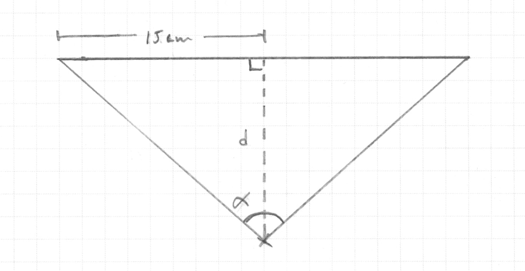
It’s not perfect, but it works:

d_h d_v α_h α_v FOV_h FOV_v
Pixel 2 24.5cm 32cm 31.47° 25.11° ~63° ~50°

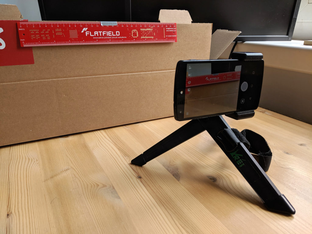
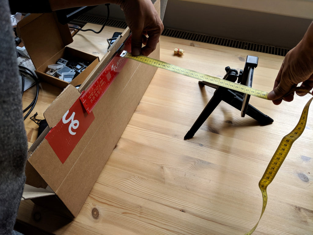
I took a 30cm ruler and taped it up, then measured how far away the camera needed to be from the ruler to fit the whole thing just inside its Field of View.

d_h = the distance away from the ruler in landscape mode
d_v = the distance away from the ruler in portrait mode

This is what it looks like:

The trigonometry for a right angle triangle means that:

α_h = arctan(15 / d_h) = arctan(15 / 24.5)
α_v = arctan(15 / d_v) = arctan(15 / 32)

and obviously the full FOV_h and FOV_v are double that.

This works with any camera, so if you don’t have the sensor size and don’t want to run through the lens equation, try this method out instead.

Finally, a practical use for all that trigonometry I memorized in high school. (Ok, that’s not true, we used a ton of it in electrical engineering, too.)

In other words, all that the Field of View triangle is saying (and indeed what the tangent ratio is saying) is that:

If we’re holding the camera in landscape mode, then stepping forwards or backwards by 24.5cm will remove or add 30cm of the scene in front of us to the picture.

If we’re holding the camera in portrait mode, then stepping forwards or backwards by 32cm will remove or add 30cm of the scene in front of us to the picture.

STM32 Virtual COM Port Issues

For some reason, the Virtual Com Port (VCP) drivers for STM32 chips were acting up and not properly enumerating a usable COM port on Windows when I was testing an STM32L476 chip.

I’m not sure if this is a chip-specific issue or if this problem shows up on more chips using the STM32Cube Hardware Abstraction Layer.

(Even after I installed Atollic TrueSTUDIO and the older STSW-LINK004 Windows utility, which I like better than the new STM32CubeProgrammer because it doesn’t require Java.)

Continue reading STM32 Virtual COM Port Issues

EAGLE CAD Custom Parts Gotchas

Here are some notes and reminders to myself, things to double and triple-check when creating a custom part.

These are things that I’ve messed up.

Package Creation

EAGLE Layers

Top (or Bottom) means exposed copper on the board, use the “Land Pattern” information in the datasheet to create these pads:

Land pattern = the exposed copper

tStop (bStop) means no colored solder mask applied in this area, so the copper is cleanly exposed, usually a bit larger than the copper pads:

qfn24-solder-mask-is-tstop

tCream (bCream) shows the size of the stencil openings, usually a bit smaller than the size of the copper pads:

qfn24-stencil-is-tcream

Note that the dimensions of tStop > Top > tCream, which makes sense. tCream is the smallest, because you usually actually don’t want your solder going all the way to the edge of the exposed copper. You get short circuits that way.

The tCream Stencils Are Usually Pretty Messed Up

One huge issue encountered quite frequently when using SMD parts in EAGLE is that the tCream pad sizes simply put too much solder paste onto the board.

tcream-equals-pad-size

People need to remember to adjust their device Packages and shrink the tCream rectangles, particularly for large pads that could cover a lot of paste and cause shorts under the package.

The default SMD part in EAGLE has tCream covering the entire pad, which will probably be a problem.

You can use the Design Rule Check -> Masks -> Cream setting to shrink the size of the stencil by some amount, but it’s not clear that this is the most effective way to design the stencil. It may require more specific, per-Package tuning. Using the DRC setting applies the rules to all SMD devices in the design.

drc-cream-change

But this doesn’t make sense, for instance, for simple devices like a 0805 resistor or capacitor, as having a lot of solder most likely will not cause a reflow short to occur.

And using these settings may cause problems for certain 3-terminal SMD chips.

Grid Units and Size

When creating surface-mount part packages, go to the command-entry bar (which might be in inches):

EAGLE CAD Grid Default

And type:

grid mm; grid alt mm;

And the system will then be thinking in millimeters:

EAGLE CAD Grid Default (mm)

You might want to set the grid to match the grid pattern in the datasheet. Let’s say you’re creating a VQFN12 part, with a 0.5mm pitch:

Land Pattern VQFN12

Then you can see that each pin center is offset by 0.5mm. So you can tell EAGLE CAD to set up a grid and alt grid this way by saying:

grid mm 1; grid alt mm 0.5;

Through-Hole Pads

When creating a through-hole via / pad it doesn’t automatically create a tStop mask that can be easily soldered to. I’ve gotten bit by this. It will create a plated through-hole, but not a copper pad. This is evil.